Equipment
SITRI has a wide a range of on-site test and verification equipment that allow us to offer reverse analysis services. With this ability, SITRI has turned what has traditionally been time-consuming experimental research into an efficient commercial service.
Our experienced technical team has deep expertise in IoT-related disciplines. So they can provide fast, efficient service for enterprises and research institutions alike.
Engineering lab’s equipment and capabilities include:
-
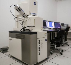
SEM + EDS
A scanning electron microscope (SEM) produces images of a sample by scanning it with a focused beam of electrons. The electrons interact with atoms in the sample, producing various signals that can be detected and that contain information about the sample’s surface topography and composition. Energy-dispersive X-ray spectroscopy (EDS, EDX, or XEDS), is an analytical technique used for the elemental analysis or chemical characterization of a sample.
-
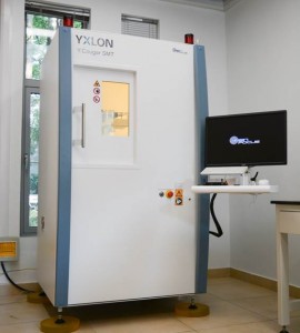
X-Ray + CT
X-ray detection is the most common method of defect detection. It can find the internal structure of a sample by non-destructive testing. 3D CT can scan the sample and detect the failure point from any angle.
-
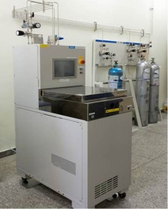
Reactive-ion Etching (RIE)
Reactive-ion etching (RIE) is a technology used in micro fabrication. It uses chemically reactive plasma to remove material deposited on wafers. The plasma is generated under low pressure (vacuum) by an electromagnetic field. High-energy ions from the plasma attack the wafer surface and react with it.
-
Ion Beam Cutter
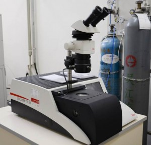
With ion beams generated via excitation of ion gun, the ion beam cutter bombards a sample lengthways perpendicular to the side of the sample, thus obtaining high-quality stress-free “cut” sections for SEM observation.
Main uses: Sample sections are obtained to provide sample preparation for detection by scanning electronic microscopy (SEM), microprobe analysis (EDS, WDS, Auger, EBSD) and atomic force microscopy or scanning probe microscopy (AFM, SPM).Scope of application: Soft/hard composite samples, samples with pore structure, heat sensitive, brittle and heterogeneous samples.
-
MEMS Wafer Testing System
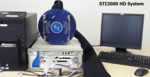
STI3000 testing system drives the mobile structures of MEMS devices through electric signals, and may keep real-time data record of capacitance change resulting from the movement of mobile structures at a maximum sampling frequency of 1MHZ and can obtain electrical performance parameters and physical performance parameters of wafer-level products by processing time domain data CC+ compiled Fourier transform program and other mathematical functional libraries.
-
8” Automatic Probe Station
The UF200R automatic probe station performs fully automatic cassette to cassette testing, GPIB interface, and full wafer mapping capabilities with a stepping error of less than 4um. The UF200R features automatic probe alignment, ink dotting and wafer mapping, and supports 4, 6, or 8″ wafers.

-
Analog Signal Tester
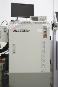
STS8200 realizes diverse product tests by configuring different test functional boards. It provides 8-channel, 5MHz digital interface and also provides up to 40V/10A and 1000V/10mA DC testing capability and 18-digit double channel power meter and time measurement unit. Through C++ programming, test programs of products under the category of big digifax and small numbers are developed. Mass production tests may be realized in combination with sorting machine or automatic probe station.
Main uses: The device completes automatic tests and feeds back test data through compiled test programs and communication interfaces.
Scope of application: LED driver, DC-DC, AC-DC, LDO, Analog Switch parameter tests.
-
MEMS packaged device testing system
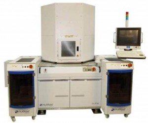
The Multi-test InGyro testing system automatically feeds packaged devices into the system and mounts them on special fixtures before sending to the test chamber. By using different excitation sources, the system generates different testing environments within the test chamber. Motion tests include overturn, rotation and acceleration as well as magnetic field, ambient pressure, humidity and temperature. Test results are automatically fed to the tester for test report generation.
Main uses: Automatic test of WLCSP and other packages of MEMS products and provision of test data.
Scope of application: Finished product tests of accelerometer, magnetometer, gyroscope and pressure sensor.
-
IGBT Static and Dynamic Parameter Tester
The Lemsys TRDS testing system can provide IGBT, MOSFET single-chip test and module test, and conducted dynamic & static parameter tests and avalanche test of products as well as seamless test of short-circuit current through integrated test modules. Test interface can provide ON-OFF waveform graph of products, and test items comply with IGBT international standard IEC60747-9.
Main uses: Automatic test of dynamic and static parameters of IGBT products, test waveform feedback, test data feedback.
Scope of application: IGBT, MOSFET chip and module parameter tests.
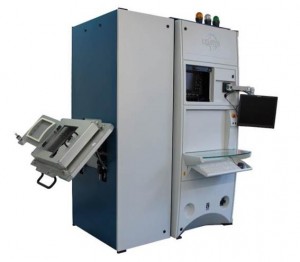
-
TIMARIS
The TIMARIS is the only PVD platform designed from its inception in 2002 to meet MRAM/STT-RAM as well as TFH development & production requirements. The TIMARIS is designed as modular PVD platform to meet all customer requirements from Semiconductor Pilot-to Mass production as well as advanced R&D. To configure a customized TIMARIS a wide range of process modules are available. The core piece of a TIMARIS is typically an MTM or FTM.

-
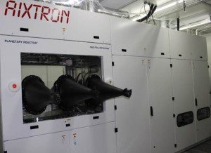
AIXTRON
MOCVD G5+: As the latest product, AIX G5+, AIXTRON SE has introduced a 5×200 mm GaN-on-Si (Gallium Nitride on Silicon) technology package for its AIX G5 Planetary Reactor platform. Following a customer-focused development program, this technology was designed and created in AIXTRON’s R&D laboratory and consists of specially designed reactor hardware and process capabilities. It is a very promising choice to meet future high performance and low cost requirements.
